Order from E-TekNet USA Headquarter
with 100% Owned PCB/PCBA Fabs in China
3 Reasons to Order PCB and PCBA from E-TekNet
High Quality Low Price
E-TekNet is the only USA PCB company that owns 100% PCB/PCBA fabs in China. Receive direct support from our USA office with added support from our fabs. We stride to provide you with the best quality and support while you enjoy our low prices.
PCB and PCBA online quote
Instant online quote for Printed Circuit Board, Solder Stencil, and PCB Assembly with live support in USA. You are just one click away from the "Online Order" and "Online File Upload". Email or give us a call with your inquiries (Hablo Espanol).
Trust, Reliable and Guarantee
E-TekNet provides PCB and PCBA service to customers together with absolute trust, reliability, quality and service guarantee. Why is it so important? Because we were cheated by a supplier before and suffered big loss. We promise reliability any time every time!
E-TekNet offers
Customer Testimonials

Sarah, Zenem Corp.
You are doing an awesome job, the turn time in getting quotes back to me is outstanding. The quality of the boards is great! I have no complaints at all. You definitely get most of our business because of the fast turn!

John, Ph.D., Sanker International, Inc.
The service and a pleasant attitude have been welcomed to our company. I appreciate your technical capabilities patients in listening to please and meet our needs and requirements, and they’re follow-up was second to none.

Carl, Sable Systems International
I have been purchasing my Bare boards from E-tek for several years, I have never had a problem with quality, Lead times, or customer support.

Craig, Coleman Air, Inc
E-Teknet is a true find. After our previous supplier went up on the price by more than 10%, we decided to look around. I can say, that turned out to be a real blessing in disguise! Yes, E-Tecknet is considerably less costly, but even more so, the level of service is simply unmatched. Turn around times are always on time and the quality is 2nd to none. A big thanks to all at E-Technet.
Quality SystemsISO9001 certified and UL certified
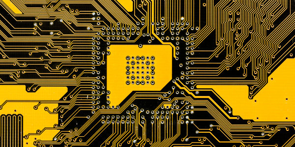
Our Capability on Bare Board PCB
Please check PCB Glossary for reference. Please contact us if you have a special requirement not listed in the following table.
| Feature | Capability |
|---|---|
| Maximum Board Layers | Up to 18 layers |
| Maximum Board size | 25" x 17" |
| Board thickness (multilayer board) | Maximum:0.13" (any layers) ; Minimum: 0.025" (4 layer) |
| Board thickness (1 or 2 layer board) | 0.02", 0.031", 0.039", 0.047", 0.062", 0.078", 0.094", 0.118", 0.125" |
| Tolerance of board thickness | +/- 10% |
| Base materials | FR-4, FR-406 (Tg 150 deg C), FR-408(Tg 170 deg C), G10, CEM3, Rogers, alumina ceramic |
| Copper weight and minimum trace width/space required | 0.5 oz (min. trace width/space 4 mil), 1 oz (min. trace width/space 5 mil), 2 oz (min. trace width/space 7 mil), 4 oz (min. trace width/space 14 mil), 6 oz (min. trace width/space 20 mil), 8 oz (min. trace width/space 40 mil) |
| Minimum conductor width and space | 0.003" (0.075 mm) for conductors including trace and annular ring |
| Minimum finished hole size | 0.006" (0.15mm). (Please see our drill sizes in stock) |
| Silkscreen/Legend colors | white, yellow, black, pink, red |
| Solder Mask (LPI) | Colors: Green, Black, Red, Blue, Purple, Yellow, Silver, Gold |
| Maximum hole aspect ratio | 10:1 |
| Surface plating | Tin/Lead HAL, immersion gold (soft gold), electrolytic gold (hard gold), immersion tin, immersion silver, OSP |
| Gold finger | Electrolytic gold on nickel: Max gold thickness 1.25 mm (30 micro-inches) |
| Blind/buried vias | Yes |
*Definition for standard features for bare board PCB : Finished PCB thickness 0.062", FR4 material, 1 oz finished copper thickness, minimum conductor width/space >= 6 mil, , minimum annular ring >= 6 mil, minimum finished hole size >=12 mil. HASL Tin-lead or HASL Lead free, green LPI soldermask, white silkscreen. For promotion prices, minimum board size 1 inch on either width or length, maximum board size 12 inches on either width or length, maximum board area 35 square inches.
*Definition for nonstandard features for bare board PCB: Any features not listed on above definition are non-standard features
Our Capability on PCB Assembly
Please check PCB Glossary for reference. Please contact us if you have a special requirement not listed in the following table.
| Feature | Capability |
|---|---|
| Minimum passive component size | 0201 |
| Minimum pitch size on BGA components | 0.4 mm |
| Parts procurement | Kitted or turnkey |
| Solder types | Tin/lead reflow or lead free RoHS compliant reflow |
| Conformal coating | Yes |
| Stainless solder steel stencil | Frameless or framed. |
| Functional test after assembly | Yes. Need customer to send over test fixture or test design. |
*Definition for standard features for PCB assembly : Minimum passive component size 0603, Minimum BGA pitch size 1.0 mm, parts received on 2nd day after order is received, lead time is 15 business day or longer
*Definition for nonstandard features for PCB assembly : Any features not listed on above definition are non-standard features
Customer Online Tools Live Demo
Click here for more customer support live demos
Tutorial on PCB and PCBA quote
Simple quote on Standard PCB
Technical terms in PCB quote
Limits on bare PCB quote
PCB assembly quote introduction
Technical terms in PCBA quote
Simple quote on Standard PCB
Limits on bare PCB online quote
Simple quote on PCBA quote
Retrieve PCB quote from account
 More tutorials on PCB/PCBA quote...
How to generate Gerber files
Generate Gerber from Protel
Generate Gerber from Eagle
Gerber file extensions
Generate BOM from Eagle